Introduction
News that Meta is exploring Google’s TPUs sent a quiet shockwave through the tech industry. For years the narrative was simple. If you wanted to do serious AI work you bought NVIDIA. You paid the “green tax.” You waited in line for H100s.
But the monopoly is cracking. The industry is waking up to a reality that Google engineers have known for a decade: general-purpose hardware is inefficient at scale.
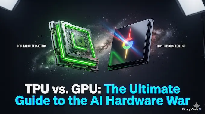
We are witnessing a fundamental divergence in computing philosophy. It is a battle between the flexibility of the Graphics Processing Unit (GPU) and the ruthless efficiency of the Tensor Processing Unit (TPU). This isn’t just a spec sheet comparison. It is a strategic fork in the road for the future of AI hardware.
This guide cuts through the marketing noise. We will dissect the architecture, analyze the economics of TPU vs GPU, and answer the billion-dollar question: Who will power the next generation of intelligence?
Table of Contents
1. What is a GPU? The General-Purpose Powerhouse That Started It All
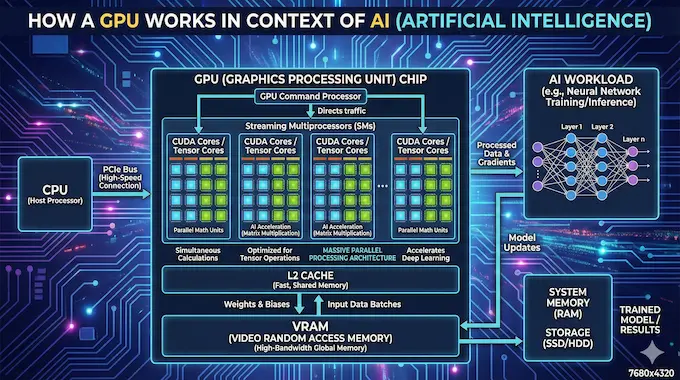
To understand the TPU vs GPU dynamic you have to look at where we started. The GPU was never meant to be the engine of artificial intelligence. It was built to render polygons for Quake and Crysis.
A Central Processing Unit (CPU) is a latency-optimized machine. It wants to finish one task as fast as possible before moving to the next. It is smart but serial. A GPU is throughput-optimized. It is a massive parallel machine designed to paint millions of pixels simultaneously.
This architecture turned out to be a happy accident for deep learning. Neural networks are essentially massive stacks of matrix multiplications. Calculating the color of a pixel and calculating the weight of a neuron look remarkably similar in terms of math. NVIDIA realized this early. They didn’t just sell chips; they built a software layer called CUDA that allowed developers to talk to these graphics cards without writing graphics code.
Today the GPU is the Swiss Army knife of computing. It can render a video game, mine a cryptocurrency, simulate a weather system, or train a Large Language Model (LLM). This flexibility is its greatest strength. It is also its Achilles’ heel. Because it tries to do everything it carries silicon baggage, logic for graphics rasterization and display engines, that deep learning simply does not need.
2. What is a TPU? Google’s Custom-Built AI Accelerator

Google saw the computational cliff coming back in 2015. They realized that if every user on Android used voice search for three minutes a day, Google would need to double its global data center footprint just to handle the compute. That was economically impossible.
So they built an ASIC. An Application-Specific Integrated Circuit.
The Google TPU is not a general-purpose computer. You cannot run Windows on it. You cannot play Cyberpunk 2077 on it. It is designed to do one thing: multiply matrices for neural networks.
The magic of the TPU lies in the Matrix Multiply Unit (MXU). In a CPU or GPU, you typically fetch data from memory, do a calculation, and write it back. This moving of data costs time and energy. The TPU uses a “systolic array” architecture.
Imagine a bucket brigade. Data flows into the chip and passes from one processing unit to the next in a rhythmic heartbeat (systole). It performs operations as it flows through the chip without constantly accessing memory. This drastically reduces the “Von Neumann bottleneck” that plagues traditional architectures.
When you strip away the graphics hardware and optimize purely for tensor math you get AI accelerators that offer massive performance per watt. This efficiency is the heart of the TPU vs GPU conflict.
3. The Core Architectural Debate: Flexibility vs. Hyper-Specialization
The engineering debate on TPU vs GPU comes down to a classic trade-off: programmability versus efficiency.
3.1 The Case for the GPU (Flexibility)
Research is messy. New model architectures appear every week. Transformers took over the world, but Mamba or some new state-space model might be next.
GPUs are programmable. If you invent a weird new layer type or a custom activation function, you can write a CUDA kernel for it and run it on an NVIDIA H100 immediately. This makes the GPU the undisputed king of research and development. It is the safe bet. You know your code will run. This is why AI hardware discussions usually start and end with NVIDIA.
3.2 The Case for the TPU (Specialization)
Production is about economics. Once you have trained a model and you are serving it to a billion users, you stop caring about flexibility. You care about cost per token and joules per query.
The TPU sacrifices programmability for raw throughput. It is harder to program low-level kernels for TPUs compared to GPUs. But if your workload fits into standard TensorFlow or JAX operations, the TPU screams. It allows you to connect thousands of chips into “TPU Pods” via super-fast interconnects, effectively creating one giant supercomputer.
If the GPU is a Formula 1 car that can handle any turn, the TPU is a dragster designed to go in a straight line faster than anything else on earth.
4. Performance Showdown: The Economics of Training vs. Inference
When analyzing TPU vs GPU performance, we must split the discussion into two distinct phases of the AI lifecycle: training and inference.
4.1 Training: The Historic GPU Stronghold
Training a massive model like GPT-4 requires immense flexibility. You are constantly checkpointing, adjusting hyperparameters, and dealing with convergence issues. Historically, GPUs owned this space. The NVIDIA software stack is mature. If a training run crashes, you can debug it easily.
However, the gap is closing. Google Gemini was trained on TPUs. This proves that AI accelerators are now mature enough to handle the most complex training workloads in the world. The TPU vs GPU gap in training is no longer about capability; it is about ease of use.
4.2 Inference: The TPU’s Home Turf
This is where the math changes. Inference (running the model) happens millions of times more often than training.
For companies like Meta or Google, a 10% efficiency gain in inference translates to hundreds of millions of dollars in saved electricity and hardware. The TPU’s systolic array architecture shines here. It delivers high throughput with lower latency.
If you are a startup doing R&D, stick to GPUs. If you are an enterprise deploying a stable model to global users, the TPU vs GPU math starts to lean heavily toward Google’s silicon.
5. The “CUDA Moat”: Is NVIDIA’s Biggest Advantage Starting to Crack?
You cannot discuss Nvidia competition without talking about the moat.
NVIDIA’s dominance is not just about silicon. It is about CUDA. For 15 years, NVIDIA has cultivated a massive community of developers. Every library, every tutorial, and every framework is optimized for CUDA first. This “CUDA moat” is formidable. It locks companies into NVIDIA hardware because moving to a different architecture often means rewriting code.
But moats dry up.
The rise of PyTorch 2.0 and JAX is acting as a great equalizer. These high-level frameworks abstract the hardware away. A developer writes code in Python, and the framework compiles it down to the machine code. Whether that machine code targets a GPU or a TPU matters less every day.
We are moving from a “hand-coded CUDA” era to a “compiler-centric” era. As compilers get smarter, the TPU vs GPU friction decreases. The “lock-in” is becoming less technical and more about cloud availability.
6. The Game Changer: Why Google Training Gemini 3 on TPUs Is a Turning Point
The launch of Gemini 3 was more than just a model release. It was a statement of independence.
For years, skeptics argued that TPUs were only good for specific, internal Google workloads. They claimed you needed NVIDIA GPUs to train state-of-the-art Foundation Models.
Google proved them wrong. By training their flagship multimodal model entirely on TPU v4 and v5 Pods, they validated the entire stack. They showed that the hardware, the optical interconnects, and the JAX software stack could scale to tens of thousands of chips without crumbling.
This is a signal to the market. When Meta looks at Google TPU infrastructure, they aren’t looking at an experimental toy. They are looking at the battle-tested hardware that built Gemini. It validates the TPU vs GPU alternative as a reality, not a theory.
7. Ecosystem & Accessibility: Why You Can’t Buy a TPU for Your PC
Here is the catch. You can go to Newegg or Amazon and buy an NVIDIA GPU. You can put it in your basement. You can own the means of compute. You cannot buy a TPU.
Google does not sell the chips. They sell the time on the chips. To use a TPU, you must enter the Google Cloud Platform (GCP).
This creates a different kind of lock-in. With NVIDIA, you are locked into an architecture, but you can move your H100s from AWS to Azure to a private data center. With TPUs, you are married to Google Cloud.
For a company like Meta, this is a complex strategic calculus. Using Google TPU infrastructure might be cheaper and faster, but it means relying on a direct competitor for your most critical infrastructure. The TPU vs GPU decision is often made in the boardroom, not the server room.
8. The Verdict in 2025: A Clear Decision Framework
The market is flooded with AI accelerators, but the choice usually narrows down to these two giants. Here is how to navigate the TPU vs GPU decision in 2025.
TPU vs GPU: 2025 Hardware Comparison
| Factor | NVIDIA GPU (H100/Blackwell) | Google TPU (v5p/Trillium) |
|---|---|---|
| Primary Philosophy | Flexibility & General Purpose | Efficiency & Specialization |
| Best Use Case | R&D, Diverse Workloads, Small scale | Large-scale Training & Inference |
| Software Stack | CUDA (Mature, dominant) | JAX / XLA (Rapidly growing) |
| Availability | Everywhere (Cloud + On-prem) | Google Cloud Only |
| Memory Bandwidth | High (HBM3e) | High (optimized interconnects) |
| Networking | InfiniBand / NVLink | ICI (Inter-Chip Interconnect) |
TPU vs GPU: Strategic Decision Guide
| If your goal is… | You should choose… | Why? |
|---|---|---|
| Training a new architecture | GPU | Maximum flexibility to debug and iterate. |
| Running stable inference at scale | TPU | Better cost-performance and energy efficiency. |
| Using legacy codebases | GPU | Likely heavily dependent on CUDA libraries. |
| Training massive LLMs from scratch | TPU (or GPU) | TPU Pods offer incredible scaling, but GPUs are standard. |
| On-premise deployment | GPU | You cannot buy TPUs for your own data center. |
9. Conclusion: The AI Hardware War Has Just Begun
The era of the monolithic AI market is over. The TPU vs GPU war is not a zero-sum game. It is a diversification of the supply chain.
NVIDIA will remain the default for years to come. Their velocity and the depth of the CUDA ecosystem ensure they are the standard for innovation. But the CUDA moat is no longer a prison wall. It is just a fence.
Google has proven that a vertically integrated approach—designing the chip, the interconnect, the data center, and the model together—yields results that general-purpose hardware struggles to match.
For the developer, this is good news. Competition drives prices down and innovation up. We are entering a world where TPU vs GPU is just an implementation detail defined by a compiler flag.
The hardware is getting faster. The software is getting smarter. And for the first time in a decade, there is a real choice on the menu. Choose wisely.
Are you planning to migrate a workload from CUDA to JAX? Let me analyze your codebase and suggest a migration strategy.
Q1: Which is better for AI, a TPU or a GPU?
The choice between a TPU vs GPU depends entirely on your specific workload stage. GPUs are generally better for research, development, and irregular workloads because of their flexibility and broad software support (CUDA). TPUs, however, are superior for large-scale production environments. They offer significantly higher energy efficiency and lower cost-per-query for stable, massive workloads like training foundation models or serving inference to millions of users.
Q2: Are TPUs a real threat to NVIDIA’s dominance?
Yes, TPUs represent the first credible “existential threat” to NVIDIA’s monopoly in the high-end AI market. While NVIDIA dominates the general market, the success of Gemini 3 proves that hyperscalers (like Google and potentially Meta) can bypass NVIDIA entirely for their most critical and expensive workloads. This validates the TPU as a battle-tested alternative that offers freedom from the “NVIDIA tax” and supply shortages.
Q3: What is the main difference between how a TPU and a GPU work?
Think of a GPU as a Swiss Army knife: it is versatile, programmable, and handles many different tasks (graphics, simulation, AI) by moving data back and forth to memory. A TPU is like an industrial apple corer: it is an ASIC (Application-Specific Integrated Circuit) built for one math operation—matrix multiplication. It uses a “systolic array” architecture to pass data directly between chip components like a bucket brigade, drastically reducing latency and power consumption.
Q4: Why did Google train Gemini 3 on TPUs if GPUs are so popular?
Google trained Gemini 3 on TPUs to prove a strategic point: vertical integration wins at scale. By designing the chip (TPU v5/v6), the data center interconnects, and the software (JAX) together, Google achieved efficiency levels that off-the-shelf GPU clusters struggle to match. It demonstrates to the market that they are self-reliant and that their “Ironwood” infrastructure is capable of handling the world’s most demanding AI training run without a single NVIDIA chip.
Q5: What is the “CUDA Moat” and can TPUs actually get around it?
The “CUDA Moat” refers to NVIDIA’s 15-year head start in software tools and developer loyalty, making it hard to switch away from their hardware. However, this moat is drying up due to modern compilers and abstraction layers like PyTorch 2.0 and JAX. These tools allow developers to write code once in Python and run it on either a GPU or a TPU, making the underlying hardware interchangeable and weakening NVIDIA’s lock-in effect.